















Next-level Wavefront metrology for Wafer-level optics
Fast, automated wavefront measurement of imaging quality of individual lenses, micro lenses, their tools and master molds
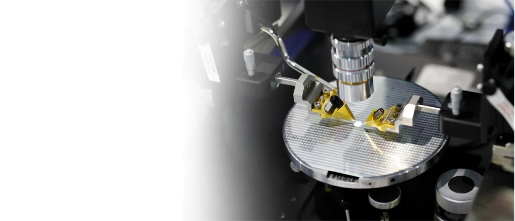
Next-level Wavefront metrology for Wafer-level optics is an application documented by Optocraft. This page summarizes the engineering task and the system-selection considerations for an Elina implementation.
Application challenge
Fast, automated wavefront measurement of imaging quality of individual lenses, micro lenses, their tools and master molds
Measurement or test approach
The optical system uses wavefront sensing and application-specific optics or illumination to quantify optical quality, alignment or laser-beam characteristics.
Topics covered by the manufacturer
- Precise and efficient
- Fast and highly-automated
- Our solution for the inspection of wafer-level optics
Information required for system selection
Define aperture, wavelength, wavefront range, spatial resolution, required accuracy, test geometry and software interface.
The problem
Fast, automated wavefront measurement of imaging quality of individual lenses, micro lenses, their tools and master molds
The method
The optical system uses wavefront sensing and application-specific optics or illumination to quantify optical quality, alignment or laser-beam characteristics.
The result
The delivered configuration must be verified against the operating envelope and performance required by the application.