









Measurement solutions for Semiconductors and electronics
Nanometre measurement in vacuum and cleanroom
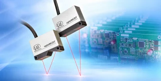
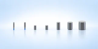
Semiconductor manufacturing equipment needs sub-nanometre resolution, vacuum compatibility and zero particle generation. Capacitive and confocal chromatic sensors deliver all three, and we integrate them with the controller and the software that records the result.
Applications
-
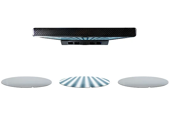
3D shape measurement of wafers
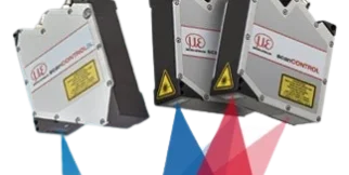
reflectCONTROL deflectometry systems are used to detect the flatness or planarity of 150 mm wafers. These measure the flatness with only one image. For this purpose, the sensors project a striped pattern onto the wafer, which is recorded by…
-
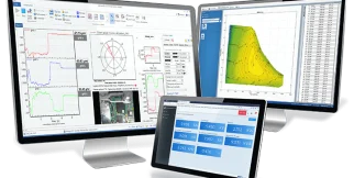
CAST 2 Cast 2 controls and monitors the measurement data from our spin tester to ensure optimal processes and quality.
CAST 2: A precise measurement and control system for spin stands. Digital interface, comprehensive process integration, and analysis.

-
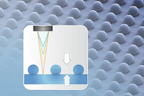
Height measurement of wafer bumps
Up to now, the 50 to 350 µm small bumps are normally inspected by camera systems during production. The decisive disadvantage of this method is that only the presence or position is checked. The height can only be determined offline, by…
-
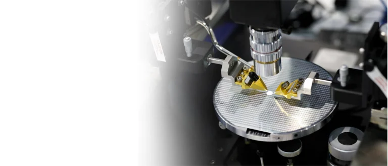
Next-level Wavefront metrology for Wafer-level optics
Fast, automated wavefront measurement of imaging quality of individual lenses, micro lenses, their tools and master molds
-
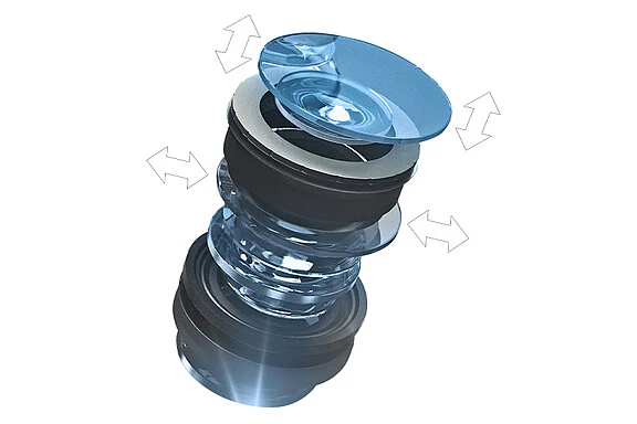
Positioning of the lens system in lithography machines
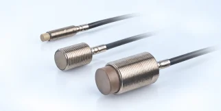
Non-contact, inductive displacement sensors (eddy current) measure the position of lens elements in order to achieve the highest possible imaging accuracy. Depending on the lens system, displacement sensors from Micro-Epsilon are used to…
-
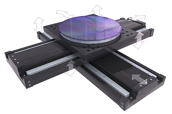
Positioning the wafer stage
Non-contact sensors from Micro-Epsilon are used for position monitoring of the wafer stage, where they measure highly dynamic XYZ movements of the stage which accelerates very rapidly. Capacitive and inductive (eddy current) sensors achieve…
-
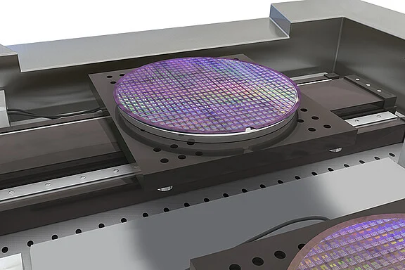
Positioning the wafer stage using capacitive sensors
Capacitive displacement sensors are used for fine positioning tasks in the wafer stage. These sensors measure the position of the stage at various points, which is particularly useful for fine alignment. Thanks to their triaxial design, the…
-
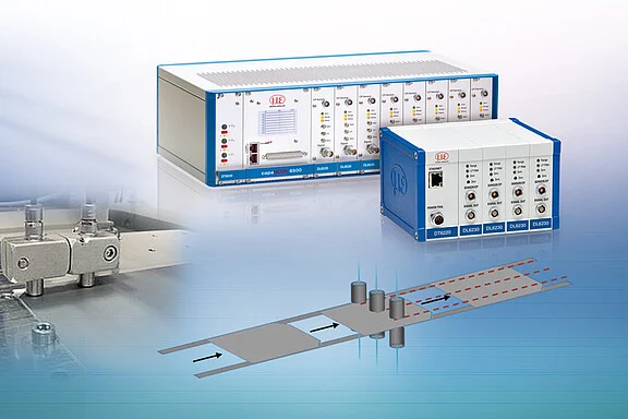
Thickness and structure measurement of solar wafers
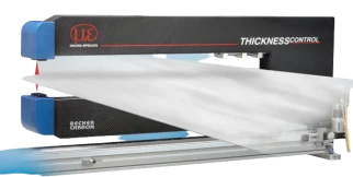
The production of solar wafers starts with the raw wafers that are sawn from the so-called ingots. These must comply with a specified thickness of about 180 µm to be processed further as a good part. The production of solar wafers starts…
-
Wafer planarity control for hybrid bonding
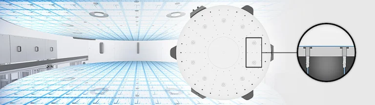
Measure wafer or die shape deviations in real time before hybrid bonding. Capacitive distance-sensor arrays scan wafer surfaces; the measurement data supports adaptive leveling and Z-axis position correction of wafer stages.
-
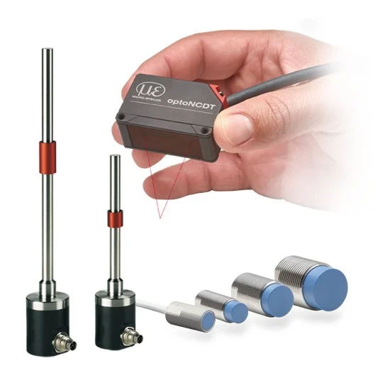
Wafer thickness and TTV
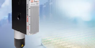
Confocal chromatic measurement of total thickness variation without touching the wafer.
-
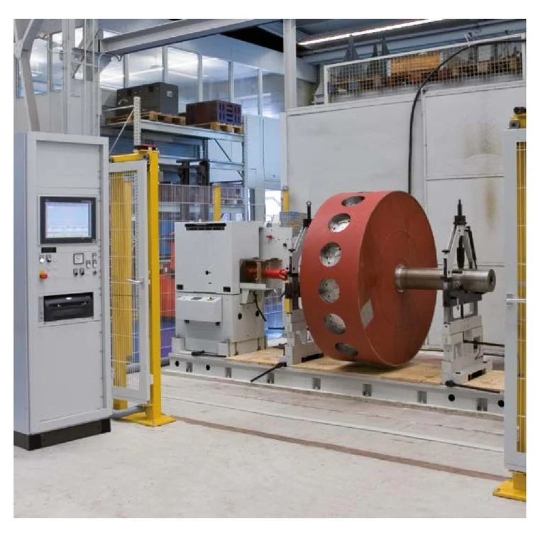
Chuck flatness
Capacitive displacement measurement at sub-nanometre resolution, vacuum compatible.
-
Stage position feedback
High-bandwidth displacement feedback for precision positioning loops.

Frequently asked questions
Answers to the most common questions about our products and services
Usually five to ten working days from when your samples reach our lab. You get a written report with the measured results and a recommended configuration.
Both. We can supply the instrument alone, or install, align, configure and prove it on your line with a measurement capability test before handover.
Documented applications include wafer planarity, shape and thickness inspection; detection of bumps, saw marks and cracks; and positioning masks, wafer stages, lenses and lithography machinery. Select a solution for the specific task and target material.
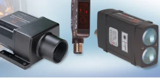
Manufacturer examples use capacitive, confocal chromatic, eddy-current, white-light interferometry, optical micrometer, profile-scanning and deflectometry technologies. Choose according to geometry, target material, process rate and operating environment.
Vacuum suitability cannot be generalized across technologies or configurations. Verify the exact model, sensor head, cable, feedthroughs and components inside the vacuum space against the process conditions.
Contact us
Tell us what you need to measure and an engineer will get back to you.
Send us a message
- Address 29 Hametzuda St., Azur Industrial Zone Azur 5800173, Israel · POB 11475
- Phone 03-5590277
- Email sales@elinatech.com
- Opening hours Sun–Thu, 08:30–18:00